Buck–boost converter
The buck–boost converter is a type of DC-to-DC converter that has an output voltage magnitude that is either greater than or less than the input voltage magnitude.
Two different topologies are called buck–boost converter. Both of them can produce a range of output voltages, from an output voltage much larger (in absolute magnitude) than the input voltage, down to almost zero.
- The inverting topology
- The output voltage is of the opposite polarity as the input. This is a switched-mode power supply with a similar circuit topology to the boost converter and the buck converter. The output voltage is adjustable based on the duty cycle of the switching transistor. One possible drawback of this converter is that the switch does not have a terminal at ground; this complicates the driving circuitry. Neither drawback is of any consequence if the power supply is isolated from the load circuit (if, for example, the supply is a battery) as the supply and diode polarity can simply be reversed. The switch can be on either the ground side or the supply side.
- A buck (step-down) converter followed by a boost (step-up) converter
- The output voltage is of the same polarity as the input, and can be lower or higher than the input. Such a non-inverting buck-boost converter may use a single inductor that is used as both the buck inductor and the boost inductor.[1][2]
The rest of this article describes the inverting topology.
Contents |
Principle of operation
The basic principle of the buck–boost converter is fairly simple (see figure 2):
- while in the On-state, the input voltage source is directly connected to the inductor (L). This results in accumulating energy in L. In this stage, the capacitor supplies energy to the output load.
- while in the Off-state, the inductor is connected to the output load and capacitor, so energy is transferred from L to C and R.
Compared to the buck and boost converters, the characteristics of the buck–boost converter are mainly:
- polarity of the output voltage is opposite to that of the input;
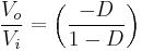
- the output voltage can vary continuously from 0 to
 (for an ideal converter). The output voltage ranges for a buck and a boost converter are respectively 0 to
  and to
  .
.
Continuous Mode
If the current through the inductor L never falls to zero during a commutation cycle, the converter is said to operate in continuous mode. The current and voltage waveforms in an ideal converter can be seen in Figure 3.
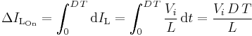
From  to
to  , the converter is in On-State, so the switch S is closed. The rate of change in the inductor current (IL) is therefore given by

At the end of the On-state, the increase of IL is therefore:
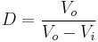
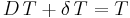
D is the duty cycle. It represents the fraction of the commutation period T during which the switch is On. Therefore D ranges between 0 (S is never on) and 1 (S is always on).
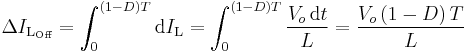
During the Off-state, the switch S is open, so the inductor current flows through the load. If we assume zero voltage drop in the diode, and a capacitor large enough for its voltage to remain constant, the evolution of IL is:

Therefore, the variation of IL during the Off-period is:
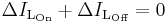
As we consider that the converter operates in steady-state conditions, the amount of energy stored in each of its components has to be the same at the beginning and at the end of a commutation cycle. As the energy in an inductor is given by:

it is obvious that the value of IL at the end of the Off state must be the same as the value of IL at the beginning of the On-state, i.e. the sum of the variations of IL during the on and the off states must be zero:
Substituting  and
and  by their expressions yields:
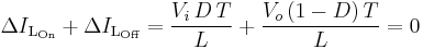
This can be written as:
This in return yields that:
From the above expression it can be seen that the polarity of the output voltage is always negative (as the duty cycle goes from 0 to 1), and that its absolute value increases with D, theoretically up to minus infinity as D approaches 1. Apart from the polarity, this converter is either step-up (as a boost converter) or step-down (as a buck converter). This is why it is referred to as a buck–boost converter.
Discontinuous Mode
In some cases, the amount of energy required by the load is small enough to be transferred in a time smaller than the whole commutation period. In this case, the current through the inductor falls to zero during part of the period. The only difference in the principle described above is that the inductor is completely discharged at the end of the commutation cycle (see waveforms in figure 4). Although slight, the difference has a strong effect on the output voltage equation. It can be calculated as follows:
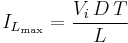
As the inductor current at the beginning of the cycle is zero, its maximum value  (at
(at  ) is
) is
During the off-period, IL falls to zero after δ.T:
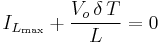
Using the two previous equations, δ is:

The load current  is equal to the average diode current (
 ). As can be seen on figure 4, the diode current is equal to the inductor current during the off-state. Therefore, the output current can be written as:
Replacing and δ by their respective expressions yields:
Therefore, the output voltage gain can be written as:
Compared to the expression of the output voltage gain for the continuous mode, this expression is much more complicated. Furthermore, in discontinuous operation, the output voltage not only depends on the duty cycle, but also on the inductor value, the input voltage and the output current.
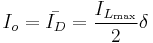
Limit between continuous and discontinuous modes
As told at the beginning of this section, the converter operates in discontinuous mode when low current is drawn by the load, and in continuous mode at higher load current levels. The limit between discontinuous and continuous modes is reached when the inductor current falls to zero exactly at the end of the commutation cycle. with the notations of figure 4, this corresponds to :

In this case, the output current  (output current at the limit between continuous and discontinuous modes) is given by:
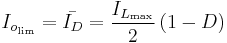
Replacing  by the expression given in the discontinuous mode section yields:
As is the current at the limit between continuous and discontinuous modes of operations, it satisfies the expressions of both modes. Therefore, using the expression of the output voltage in continuous mode, the previous expression can be written as:
Let's now introduce two more notations:
- the normalized voltage, defined by
 . It corresponds to the gain in voltage of the converter;
 - the normalized current, defined by
 . The term
  is equal to the maximum increase of the inductor current during a cycle; i.e., the increase of the inductor current with a duty cycle D=1. So, in steady state operation of the converter, this means that
  equals 0 for no output current, and 1 for the maximum current the converter can deliver.
Using these notations, we have:
- in continuous mode,
 ;
; - in discontinuous mode,
 ;
; - the current at the limit between continuous and discontinuous mode is
 . Therefore the locus of the limit between continuous and discontinuous modes is given by
 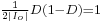 .
.
These expressions have been plotted in figure 5. The difference in behaviour between the continuous and discontinuous modes can be seen clearly.
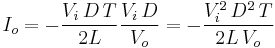
Non-ideal circuit
Effect of parasitic resistances
In the analysis above, no dissipative elements (resistors) have been considered. That means that the power is transmitted without losses from the input voltage source to the load. However, parasitic resistances exist in all circuits, due to the resistivity of the materials they are made from. Therefore, a fraction of the power managed by the converter is dissipated by these parasitic resistances.
For the sake of simplicity, we consider here that the inductor is the only non-ideal component, and that it is equivalent to an inductor and a resistor in series. This assumption is acceptable because an inductor is made of one long wound piece of wire, so it is likely to exhibit a non-negligible parasitic resistance (RL). Furthermore, current flows through the inductor both in the on and the off states.
Using the state-space averaging method, we can write:
where  and
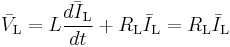
and  are respectively the average voltage across the inductor and the switch over the commutation cycle. If we consider that the converter operates in steady-state, the average current through the inductor is constant. The average voltage across the inductor is:
When the switch is in the on-state,  . When it is off, the diode is forward biased (we consider the continuous mode operation), therefore
  . Therefore, the average voltage across the switch is:

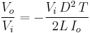
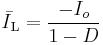
The output current is the opposite of the inductor current during the off-state. the average inductor current is therefore:
Assuming the output current and voltage have negligible ripple, the load of the converter can be considered as purely resistive. If R is the resistance of the load, the above expression becomes:
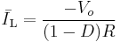
Using the previous equations, the input voltage becomes:
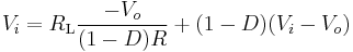
This can be written as:
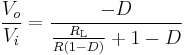
If the inductor resistance is zero, the equation above becomes equal to the one of the ideal case. But as RL increases, the voltage gain of the converter decreases compared to the ideal case. Furthermore, the influence of RL increases with the duty cycle. This is summarized in figure 6.
See also
References
Further reading
- Daniel W. Hart, "Introduction to Power Electronics", Prentice Hall, Upper Saddle River, New Jersey USA, 1997 ISBN 0-02-351182-6
- Christophe Basso, Switch-Mode Power Supplies: SPICE Simulations and Practical Designs. McGraw-Hill. ISBN 0071508589.